Get the maximum out of your technology, whatever the node
Choosing the right process node is often a complex decision for SoC designers. Whilst mature nodes give the assurance of low NRE perfectly suited for low-volume production, advanced nodes are often seen as the right path for higher volume, more complex and lower power SoC design.
With our unprecedented low-power IP catalog and SoC design experience, we help you achieve your goals with the right node, whatever your challenge.
Unique expertise in FD-SOI to boost your energy efficiency to the next level
FD-SOI
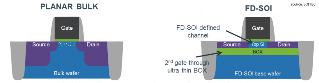
Fully depleted silicon-on-insulator (FD-SOI) relies on a very unique substrate provided by companies like SOITEC, who control their substrates’ thickness on an atomic scale.
FD-SOI presents remarkable transistor performance in terms of power, performance, and area / cost trade-offs (PPAC), making it possible to cover from ultra-low power to high-performance digital applications with a single technology platform.
In addition, FD-SOI offers a unique advantage with body bias, which gives designers the ability to mitigate process, temperature, voltage and aging variations. Moreover it offers very interesting additional features such as near-threshold supply capability, ultra-low sensitivity to radiation and very high intrinsic transistor speed, making it most likely the fastest RF-CMOS technology on the market.
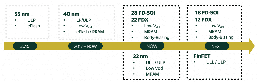
FD-SOI is currently setting new standards in many applications (automotive, 5G, IoT, space, edgeAI). FD-SOI is supported by multiple foundries and integrated device manufacturers (IDMs) with full technology offerings now available for the 28 nm and 22 nm nodes.
We acquired unique skills in FD-SOI design to help you benefit easily from the unique energy efficiency enabled by this technology. Thus, we can help you to improve the energy efficiency of your SoC by up to 7X.
Strategic partnership with all major foundries
We have been partners with many foundries over the years and received TSMC’s Open Innovation Platform® Partner of the Year Award for Specialty IP two years in a row (2014 & 2015).